


Impedance Controlled Standard Build-Ups
Impedance Controlled Standard Build-Ups
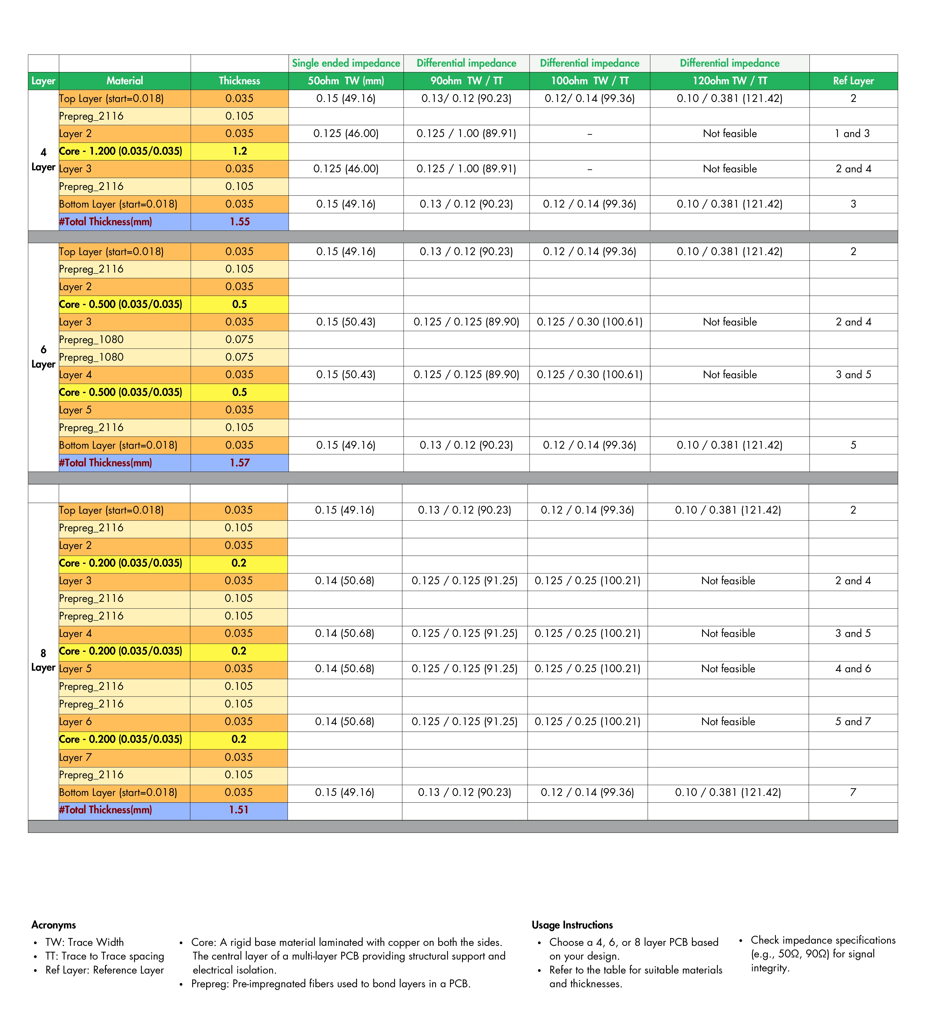
Impedance-controlled buildups are carefully structured PCB layer arrangements designed to maintain precise electrical impedance, ensuring signal integrity across high-frequency circuits. This control is crucial in modern PCB design, helping to prevent signal loss and interference, particularly in complex, multi-layer configurations.
At PCB Power, we are committed to providing industry-standard impedance-controlled build-ups for PCB fabrication. With our extensive experience in PCB manufacturing, we deliver reliable, precision-engineered stack-up configurations that meet rigorous signal integrity requirements. We recognize the critical role of consistent impedance in high-performance PCB designs, and you can count on us to uphold the highest standards of quality and reliability.
Below, you’ll find detailed specifications for our 4, 6, and 8-layer impedance-controlled build-ups. Each configuration includes precise information on layer materials, thicknesses, trace widths (TW), and trace-to-trace spacing (TT) designed to achieve specific impedance values (such as 50Ω, 90Ω, and 100Ω). These parameters are crucial in maintaining signal integrity and performance in high-frequency PCB applications.
Please Note:
- These impedance values are calculated based on high-Tg FR4 material with a dielectric constant (DK) of 4.3.
Want to explore the dielectric contants of materials we offer?
Click below to download our Master Material Data Sheet, which includes DK values for all standard materials available at PCB Power.
Click here to download Material DK Reference Sheet.
Place your order with PCB Power.
We hope this information provides valuable insights into designing PCB stack-ups that meet your project's unique requirements.
If you have any questions or need further assistance with your PCB stack-up design, please don't hesitate to reach out to our experienced support team. We’re here to help you achieve the best possible PCB configuration for your application.

